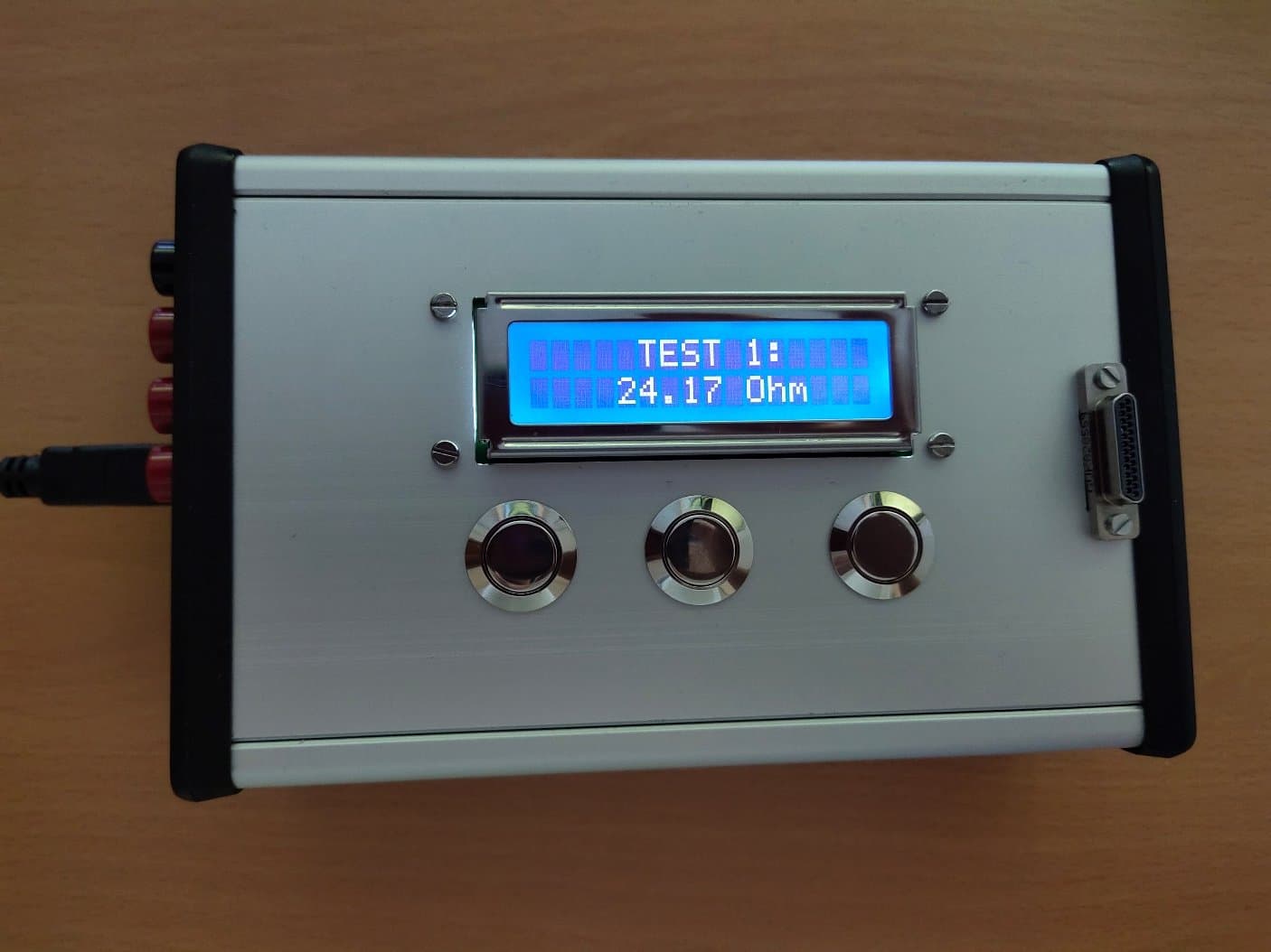
Functional Verification Device for an Electronic Subsystem
Project work at Diehl Defence: a complete Arduino-based test box that automates 34 resistance checks on an electronic subsystem — concept trade studies, custom four-layer PCB with a 32-relay switching matrix and constant-current measurement, enclosure, firmware state machine and a built-in calibration path.
34 measurements, by hand, for every single unit
During my dual-study placement at Diehl Defence, an electronic subsystem for an international project needed a functional check after assembly: 34 resistance measurements between defined pairs of pins on the subsystem's 25-pin cable — its only external interface. The target values span four orders of magnitude, from sub-1 Ω shielding and continuity checks up to winding and potentiometer paths of several kilo-ohms, each with its own tolerance band.
Until then this meant a technician with a multimeter, a pin-out table and a lot of patience: find the two pins, probe them, read the value, compare against the tolerance, write it down, 34 times per unit. That is slow, and every manual step is an opportunity for a transposed pin pair or a misread digit.
My project assignment — the T1000 project work of the DHBW dual-study programme — was to replace that procedure with a purpose-built test device: plug in the subsystem, press a button, and let the box step through all 34 checks itself. I had 13 weeks, and the explicit goal of going through every stage of an electronics development cycle: concept, review, schematic, layout, board bring-up, enclosure and software.
What the box had to do
The requirements were short but firm. Measurement accuracy had to stay inside the tolerance bands of the official test table — some of which are as tight as ±1 Ω on a nominal 0 Ω shielding path. The device had to make testing faster and less error-prone than the manual procedure. The user interface had to be simple enough for routine use in production, not just by the person who built it. And the platform was fixed: an Arduino board, partly for cost, partly because the schedule left no room for learning a new ecosystem.
One property of the test sequence shaped the whole design: during the first eight checks, the unit under test has to be brought into defined mechanical positions by hand, so those tests must run one at a time with an operator confirming each step. Tests 9 through 34 have no such constraint and can run as one automatic burst. The operating concept — one OK button pressed between the early tests, then everything else at once — falls straight out of that.
There was also a hard organisational gate baked into the process: the concepts had to be presented in a design review with the engineers responsible for the project, and only the reviewed-and-chosen concept would get built. A small taste of how development actually works in industry, which was very much the point of the exercise.
How do you measure a resistance with a microcontroller?
An Arduino cannot measure resistance — it can only measure voltage with its 10-bit ADC. So the first concept decision was how to turn 34 unknown resistances into voltages. Option one is the classic voltage divider: put a known comparison resistor in series with the unknown one across the 5 V rail and read the midpoint. It is simple and needs no extra parts, but its sensitivity collapses when the unknown resistance is far from the comparison value — covering 0.5 Ω to 7 kΩ would mean switching between several comparison resistors.
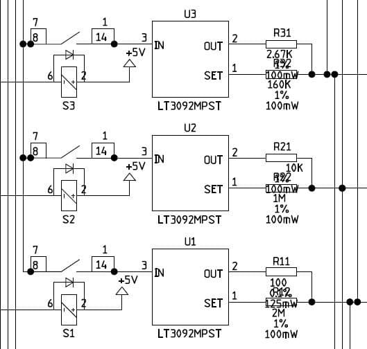
Option two is a constant-current source: drive a known current through the unknown resistance and measure the voltage drop directly, with R = U/I. That needs dedicated current-source hardware, but it has two decisive advantages. The current can be chosen per measurement range, so every value lands in a comfortable part of the ADC's 0–5 V window. And, more subtly: pushing a real current — up to 200 mA — through the connection is itself a test. A hairline solder bridge might pass a multimeter continuity check, but a path that carries 200 mA without drama is genuinely load-bearing.
That second argument won the review. The final design uses three switchable LT3092 constant-current sources — 200 mA for the low-ohm continuity and shielding checks, 1 mA and 0.6 mA for the kilo-ohm ranges — each set by a pair of programming resistors.
Routing one measurement across 25 pins
The second concept question: how does one measuring circuit reach 34 different pin combinations on a 25-pin connector? Something has to switch the current source and the ground return to the right pins for each test. I compared four options: electromechanical relays, NPN transistors, MOSFETs, and hard-wiring all combinations through shift registers.
Transistors and MOSFETs switch fast and silently, but both sit directly in the measurement path — a saturated NPN drops a few hundred millivolts, which is fatal when the thing you are measuring drops 20 mV at 200 mA. MOSFETs would also have needed gate voltages above the 12 V rail, meaning an extra step-up converter. The shift-register variant would have been quick to program but freezes the test table in copper: any future change to the test sequence would mean a new board.
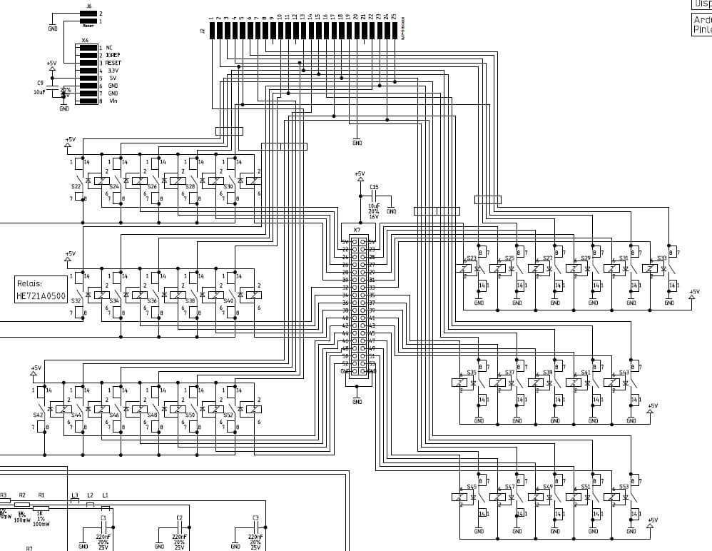
Relays won on the physics: metal contacts with milliohm contact resistance barely disturb the measurement, and a 5 V coil happily switches the 12 V measurement rail without level-shifting. The price is size — 32 relays dominate the board — plus settling delays and contact bounce that the software has to wait out after every switch. The final architecture is two banks of 16 relays: one bank connects the selected current source to the 'positive' pin of each test, the other connects the corresponding return pin to ground, all driven directly from the Arduino Mega's 32 digital outputs.
Three concepts on the table, one leaves the room
For the design review I condensed the option space into three full concepts. Option A: voltage-divider measurement with relay switching. Option B: constant-current measurement with relay switching. Option C: hard-wired shift-register routing with divider measurement. Each came with a sketch, a parts estimate and an honest list of weaknesses — including, for the display question, the glamorous alternatives of 34 individual status LEDs or a single red/green pair.
The review picked Option B, for the reasons the trade study had already suggested: the current source doubles as a load test of every connection, and adapting the current to the measurement range makes the accuracy far more uniform across four decades of resistance than any practical set of comparison resistors. For the user interface, a 16×2 character LCD beat the LED options — it can name the test, show the measured value in ohms, and give plain-text instructions, which is what 'usable in production by anyone' actually requires.
The platform choice within the Arduino family was driven by pin count: the switching matrix alone consumes 32 digital outputs, which rules out the Uno. The Mega 2560 has 54 digital I/O pins and 16 analog inputs, costs a third of a Due, and its simpler 8-bit processor was entirely sufficient for a device whose fastest event is a relay closing. Estimated parts cost of the whole box: about 180 € plus roughly 200 € for the industrially manufactured four-layer PCB.
Where the accuracy actually goes
Before building anything I estimated the error budget, term by term. Contact and transition resistances: the measurement path crosses two plug connections at up to 20 mΩ each — negligible at kilo-ohm levels, but about 4% of a 1 Ω measurement. The LT3092 holds its current to 1% per the datasheet, a flat 1% on every reading. The ADC's 10 bits give 4.9 mV steps on the 5 V range; assuming conservatively that noise costs one step, that is 10 mV on a signal of 1–5 V — well under 0.1%, effectively free.
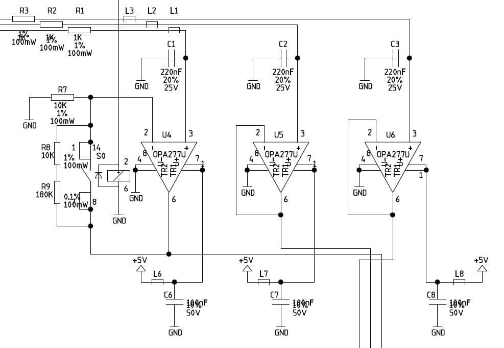
The interesting term is the relays. Their contact resistance sits directly in series with the unit under test, and it drifts with temperature and contact wear — you cannot just subtract a fixed datasheet value. The design answer is in-situ self-calibration: three precision reference resistors live permanently on the board behind their own relays. Before measuring, the box can route each current source through its reference resistor, measure the whole chain, and compare against the known value. Whatever offset appears is the resistance of the switching path itself, and it gets subtracted from subsequent measurements — reducing that error term to roughly zero by construction.
Summed up: about 5% worst-case error on the smallest 1 Ω measurements, dominated by connector transition resistance, shrinking rapidly with the measured value and dropping to essentially the 1% current-source tolerance in the kilo-ohm ranges. Comfortably inside every tolerance band in the test table.
Op-amps: buffers first, amplifiers when needed
Between the measurement point and the Arduino's analog input sit three OPA377 operational amplifiers, one per current source, and their first job is deliberately boring: unity-gain impedance buffering. The ADC input must not draw current from the measurement path — any current it sinks flows through the unknown resistance and falsifies the reading. A voltage follower with near-infinite input impedance decouples the two, and doubles as protection for the microcontroller against voltages beyond its comfort zone.
The 200 mA channel needed one extra trick. Its job includes the sub-1 Ω measurements, where even 200 mA only develops on the order of 0.1 V — using a tenth of the ADC range and amplifying every count of noise into the result. That channel's op-amp can therefore be switched by relay between gain 1 and gain 20: high gain for the very small resistances, unity gain for the rest of its range. A non-inverting amplifier with a switchable feedback network, straight from the textbook, applied exactly where the numbers said it was needed.
This is the part of the project where the sizing stopped being catalogue shopping and became actual analog design: choosing gains so that every one of the 34 expected values lands in the sweet spot of the 0–5 V window, for its assigned current source, with margin for the tolerance band on top.
One channel on perfboard before 39 relays on a PCB
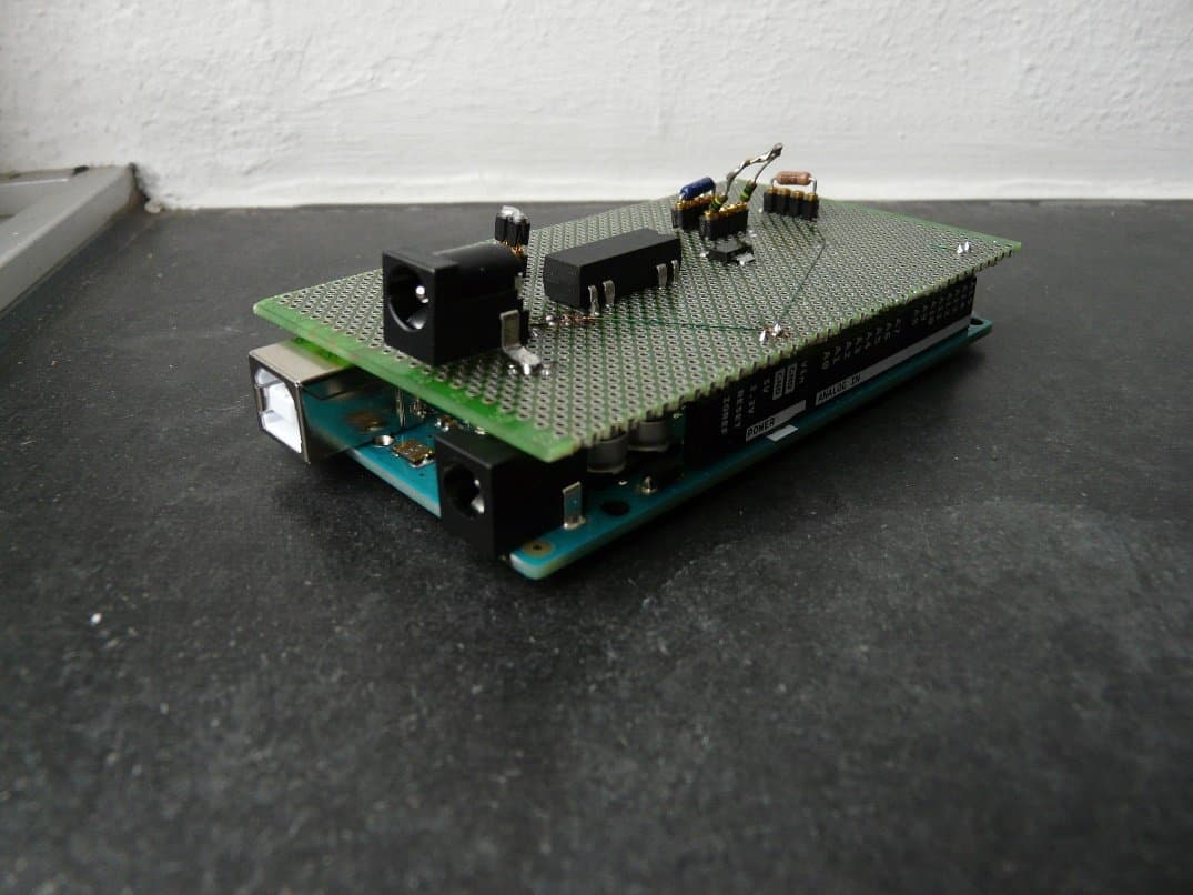
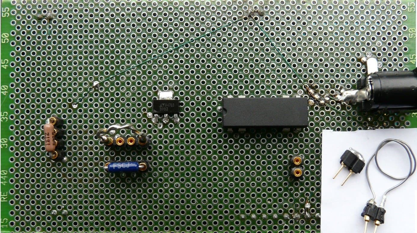
Committing a four-layer PCB to production on the strength of datasheets alone would have been brave. So week three produced a prototype shield: one complete measurement channel — current source, relay, programming resistors, op-amp — soldered onto perfboard as a stackable shield for the Mega, with jumper sockets in place of fixed resistors so values could be swapped during testing, and a wire-loop jumper in the relay coil path so a current clamp could measure the true switching current.
The prototype answered the questions it was built to ask. The measurement principle held: current source, relay path and ADC produced stable, convertible readings. And the Arduino's on-board 5 V regulator proved it could hold more than five relay coils simultaneously — comfortably above the two-to-three relays plus display that the worst-case test step actually requires, so no separate coil supply was needed.
It also settled the perfboard question definitively, in the negative: one channel was already a dense little thicket of wires. Thirty-nine relays, three current sources, three op-amp stages and a display header hand-wired on perfboard would have been a reliability lottery — and for a device whose entire purpose is trustworthy measurements, contact quality is not where you save 200 €. The PCB decision made itself.
The full schematic: everything on one A3 sheet
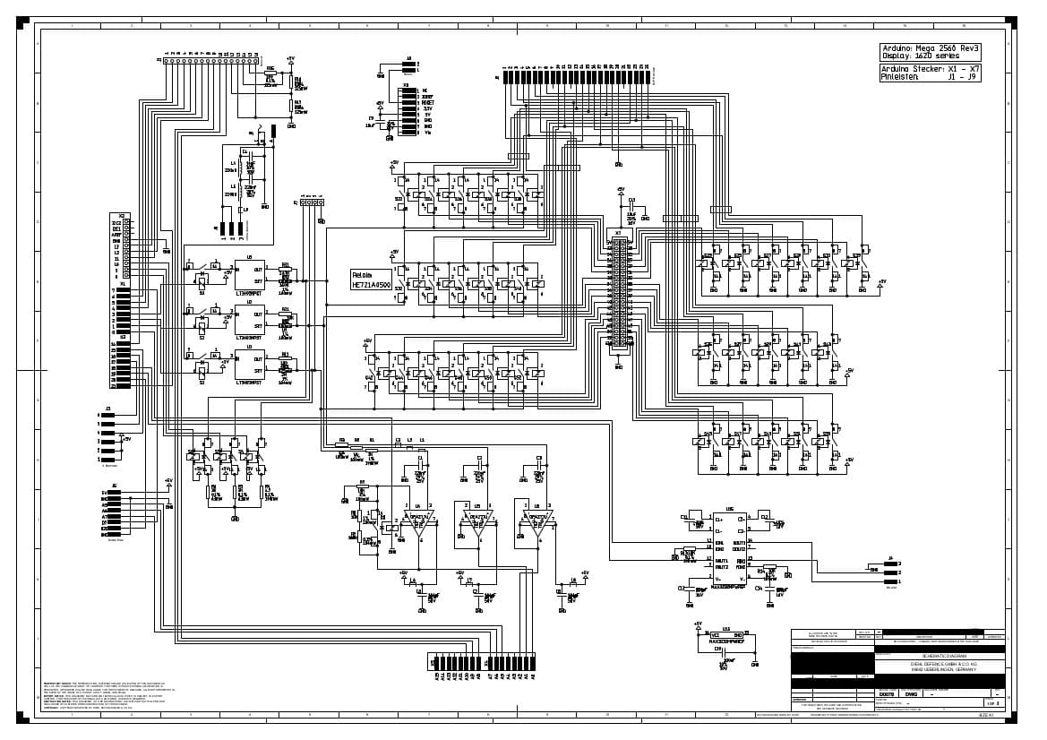
With the concept validated, the block diagram grew into a complete schematic in the company's EDA toolchain (Mentor Graphics). Around the core measurement chain came the supporting cast. A single 12 V barrel-jack input feeds the whole box; a two-stage LC low-pass with a 22 kHz corner frequency and ferrite beads cleans the switch-mode supply's output before it reaches the current sources and the Arduino — a resistance measurement is only as quiet as its supply rail.
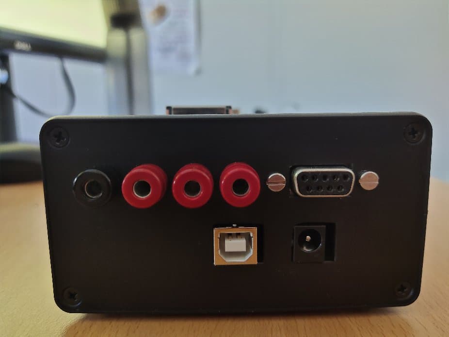
The 16×2 display hangs off a pin header with a resistor divider generating its contrast and dimming voltages. A MAX3232 transceiver converts the Arduino's UART to RS-232 levels for a D-sub connector on the back panel, so a PC can talk to the box — the hook for later firmware updates and logging. Four banana jacks on the rear panel expose the calibration interface, where reference resistors can be connected to check the whole measurement chain end-to-end.
Two pin-assignment tables tie the schematic to the test specification: for each of the 34 tests, which digital pin closes which relay, connecting which current source to which connector pin, with which return pin to ground. Those tables became the single source of truth — the same mapping lives in the firmware's measurement array, so schematic, board and software all speak the same language.
Four layers: signals outside, power inside
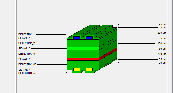
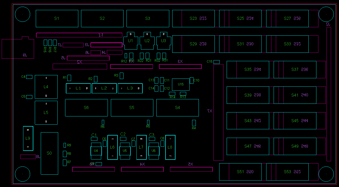
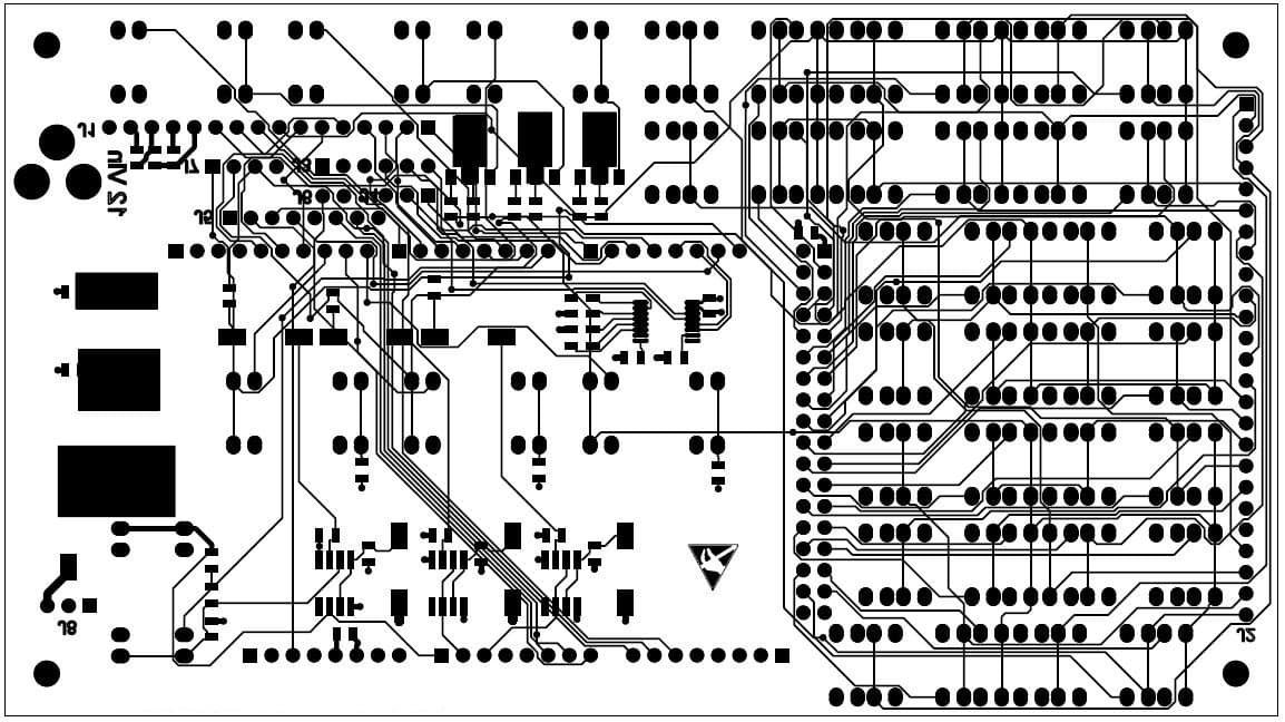
The board was fixed at 152 × 85 mm — the largest PCB the chosen enclosure can swallow — and laid out as a four-layer stack. The two inner layers are solid planes, 12 V and ground; the two outer layers carry the routed signal traces. That is the standard recipe, and the reasons it is standard applied here directly: through-hole parts like the 39 relays can tap their supply straight down into the planes with a single via, the routing layers stay uncluttered, and the tightly coupled plane pair keeps supply impedance low.
Copper thickness is a standard 35 µm all around — with 200 mA as the largest current and a relay coil as the fastest load, neither high-current nor controlled-impedance rules applied. The 12 V distribution traces that do carry the measurement current were simply drawn wider. The dielectric thicknesses were chosen mostly to land on a sensible overall board thickness, with the Vcc and ground planes kept close together in the core.
One layout decision was driven purely by mechanics: the board mounts upside-down in the enclosure, so that the Arduino and all plug-on connectors point upward and gravity works with the friction-fit headers instead of against them. The silkscreen labels are consequently mirrored on the underside — a detail that looks like a mistake in the Gerber files and is entirely deliberate.
Placement follows the schematic, routing follows Manhattan
Placement mirrors the signal flow: the right half of the board is a solid field of 32 switching relays with the 25-pin connector header at the outer edge, so the measurement paths leave the board on the shortest possible route. The current sources sit next to the power input, the op-amps between them and the Arduino's analog pins, and the headers for display, buttons and calibration jacks cluster at the top-left where their panel-mounted counterparts live in the enclosure. Four corner holes bolt the board to the case.
Routing followed a simple discipline: keep every connection within its Manhattan distance — the shortest path achievable on a rectilinear grid. Horizontal runs went preferentially onto layer 1, vertical runs onto layer 4, with vias stitching direction changes. The SMD parts forced exceptions (they only exist on layer 1, and every escape to layer 4 costs a via), but the discipline kept the dense relay field routable without a single autorouter pass.
The result came back from fabrication as a tidy four-layer board that needed no rework — every relay, header and SMD footprint fit at the first attempt. The one layout error that did slip through was invisible in the Gerbers, and it waited patiently until software bring-up to reveal itself. More on that in chapter 15.
CAD drawings, milled panels, and epoxy where it counts
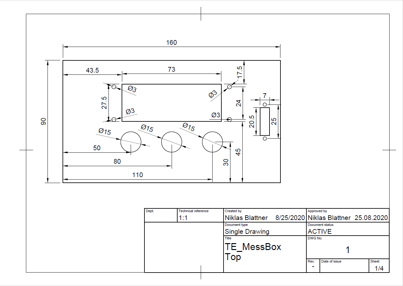
The electronics live in an off-the-shelf Hammond 1455 extruded-aluminium case, but every hole in it is custom. I modelled the front and rear panels and the lid in Fusion 360 and produced dimensioned technical drawings for the workshop: three Ø15 mm bores for the illuminated push buttons, the display cutout with its four mounting holes, and the rear-panel pattern for USB, the 12 V jack, the D-sub connector and four banana jacks.
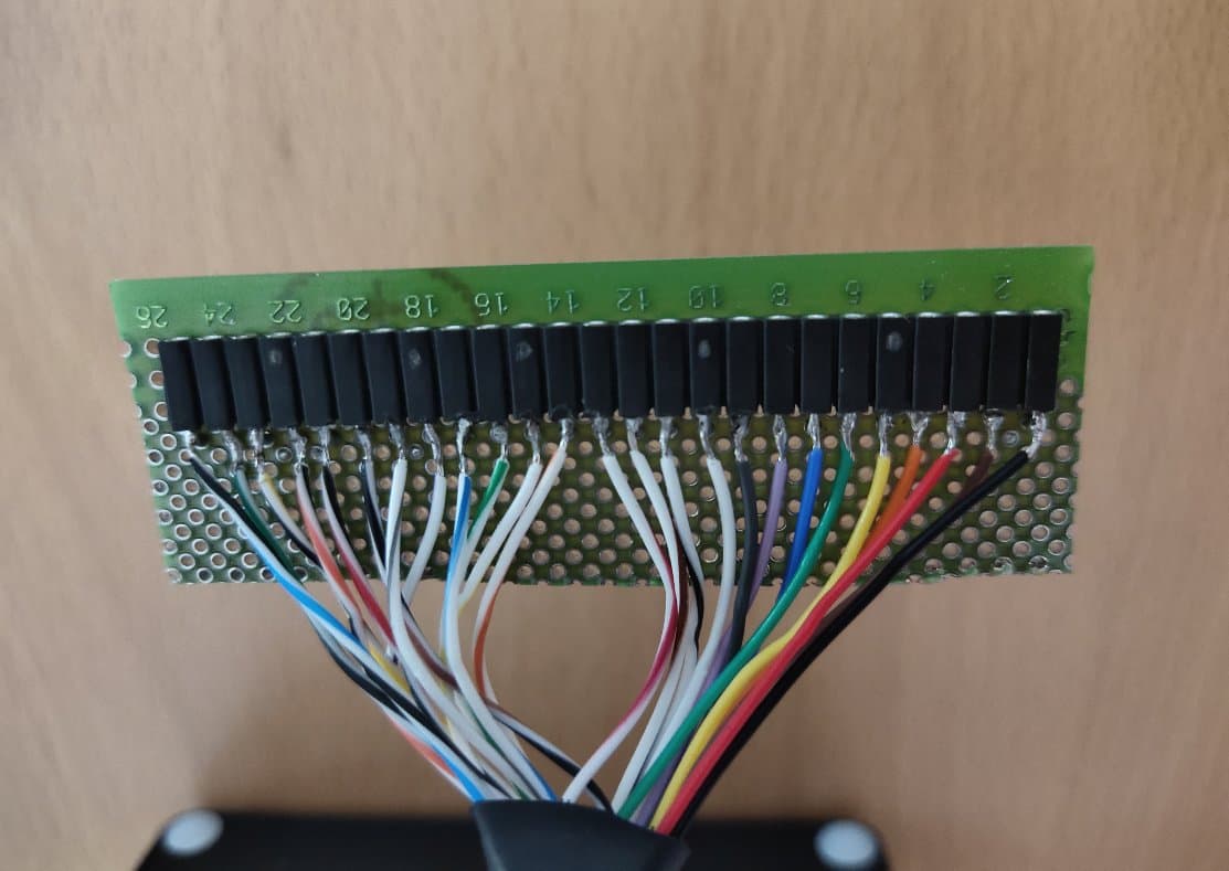
Assembly had its own small engineering problems. The display's 16-pin header takes mechanical load every time the lid is closed, so its solder joints were potted in epoxy. The 25-pin connection to the unit under test had to pass through a deliberately small panel opening — solved by splitting it into three short connector segments that thread through individually. And to make firmware development independent of real hardware, I built a test adapter that plugs into the 25-pin interface and accepts arbitrary resistors between any two pins — a fake unit under test for the desk.
The connectors inside the box are plain friction-fit headers, which works but left room for improvement I noted honestly in the report: coding the connectors (clipped pins, blocked sockets) would make cross-plugging physically impossible instead of merely unlikely.
The finished box
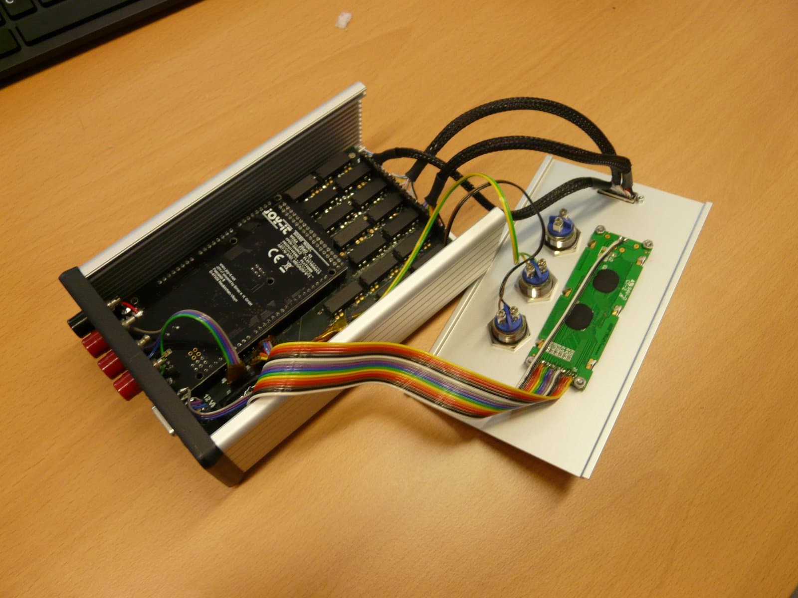
Everything together: the four-layer board carpeted with relays, the Arduino Mega stacked on its headers, ribbon cables to the lid-mounted display and buttons, sleeved wire bundles to the panel connectors. On the outside, a clean instrument: three buttons — OK, BACK, RESET — a 16×2 display, and the connector panel on the rear.
The operating concept stayed exactly as sketched in week two. Connect power and the unit under test, then step through the tests with the OK button; BACK repeats the previous measurement; RESET is wired straight to the Arduino's reset pin as an always-available escape hatch. Holding OK and BACK together at the start screen enters calibration mode, where the banana jacks and the on-board precision resistors let the whole measurement chain be verified against known values.
Total hardware cost landed around 380 € plus the project-specific connector — parts, professionally fabricated four-layer PCB and enclosure included. Set against technician time saved on every single unit tested, the payback argument was not a difficult one.
Draw the state machine before writing a line of code
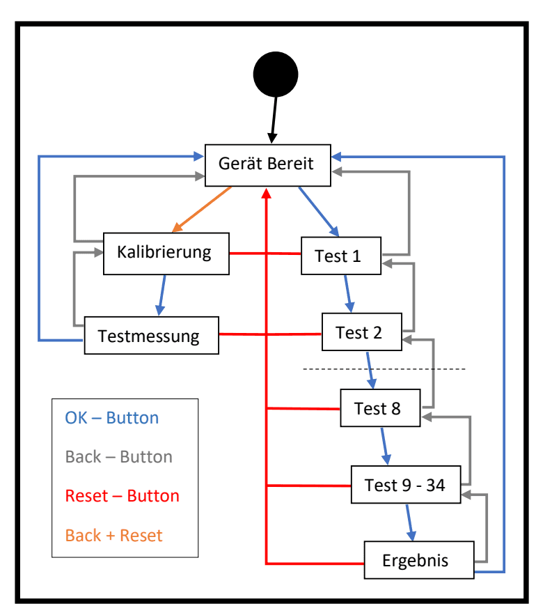
The firmware was designed on paper first. A state diagram maps every moment of operation to exactly one state: device ready, calibration, test measurement, tests 1 through 8 as individual operator-confirmed states, tests 9–34 as one automatic block, and the results screen. The three buttons are the only transitions — OK advances, BACK returns, RESET drops back to the start from anywhere. If every state has a defined exit for every button, the software cannot wedge itself into a corner an operator can't escape from.
The split between single-step and batch tests encodes the physical test procedure directly: the first eight checks need the unit under test in specific hand-set positions, so the machine waits for a human between them; the remaining 26 need nothing and run as one burst, comparing each reading against its tolerance band and stopping with an error code the moment one fails.
A use-case diagram rounded out the design stage, forcing the roles apart: the production worker who runs tests, the calibration service that verifies the device annually, the developer who maintains it. Small formalisms, but they caught requirements — like the yearly calibration check needing its own accessible mode — that pure feature-list thinking would have missed.
A lookup table, three macros, and one mirrored pin header
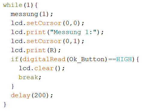
The firmware's core is deliberately data-driven: a two-dimensional array holds, for each of the 34 tests, which two relays to close and which current source to use. The measurement routine walks that array — energise the relays, wait out the contact bounce, enable the selected current source, read the ADC, convert voltage to resistance, park the result. Changing the test sequence means editing a table, not logic; exactly the flexibility that justified relays over hard-wiring back in the concept phase.
Small macros wrap every current source and the gain-switching relay in explicit on/off functions. Partly for readability, partly thermal: the current sources heat up under load, so the discipline of switching them on only for the milliseconds of an actual measurement is enforced in one place instead of remembered in twenty.
And then there is the realpin() function — my favourite bug of the project. The 34-pin header that drives the relay matrix went onto the board mirrored: commanding pin 50 fires the relay of pin 51, and vice versa, all the way down the header. Electrically perfect, mechanically unfixable without a board respin. The software fix is two lines: even pin numbers get +1, odd get −1, courtesy of the modulo operator, applied transparently for pins 22–53. The measurement table stays human-readable against the schematic, and the mirror lives in exactly one function.
A measuring device is only worth its calibration path
A test device that itself goes unverified just moves the uncertainty one box downstream, so the calibration story got the same attention as the measurement itself. Level one is automatic: the three on-board precision resistors sit behind their own relays, and the box can route each current source through its reference at any time. If the measured chain disagrees with the known value, the device flags it and requests calibration — this is also the mechanism that cancels the relay contact resistance out of every measurement.
Level two is the external interface: calibration mode, entered with OK+BACK, measures whatever is connected to the four rear-panel banana jacks. With certified reference resistors attached, the calibration service can verify the complete chain — connector, relays, current source, amplifier, ADC, conversion math — against traceable values, annually, without opening the box.
That two-level scheme is what makes the box a legitimate production tool rather than a clever student project: before release into manufacturing it goes through formal acceptance by the calibration office and quality management, and the annual verification path is designed in, not bolted on.
Every requirement met — and a wishlist for version two
After 13 weeks the box did what the assignment asked: all 34 measurements automated behind a three-button interface, accuracy inside every tolerance band of the test table, one power plug, one connector to the unit under test. Concept review, schematic, four-layer layout, board assembly, enclosure machining, firmware and calibration concept — the complete development cycle, compressed into one semester project, with the finished device headed for daily use in production after formal acceptance.
The honest lessons list from the report: code the internal connectors so they cannot be cross-plugged; add a power-indicator LED; and the mirrored pin header taught me permanently that a footprint's pin-1 marking deserves the same review attention as any net. For a version two, the natural extensions are motorised positioning of the unit under test — which would remove the human from the eight manual position steps and make the entire sequence one button press — and automatic test protocols over the already-installed RS-232 link, logging every measurement and calibration for full traceability.
As a first complete electronics project it was formative in a way coursework rarely is: every abstraction level from ADC counts to quality-management acceptance belonged to the same 13 weeks, and every decision — measurement principle, relay physics, layer stackup, state machine — had to survive contact with a real production floor.